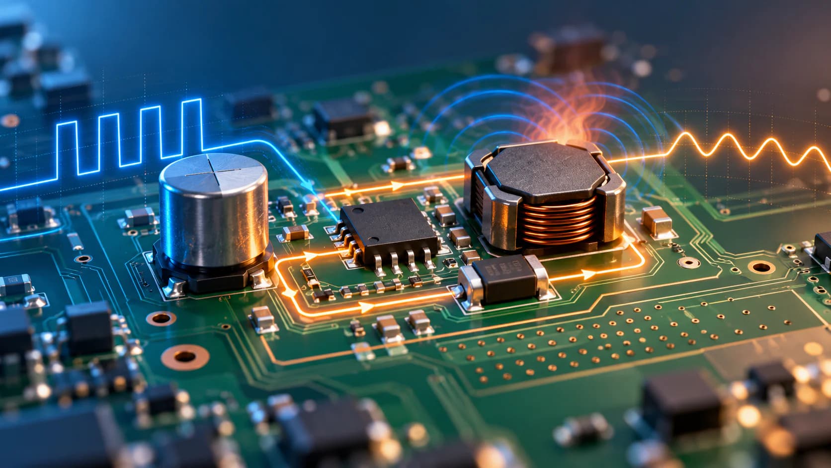
A switching power supply can have a perfectly designed schematic and carefully selected components, yet still suffer from excessive noise, unstable output voltage, EMI problems, or overheating.
Why?
Because in switching power electronics, PCB layout is part of the electrical design itself.
Unlike many low-frequency circuits, switching regulators generate fast voltage and current transitions. The physical arrangement of components, copper traces, and return paths directly affects how the circuit behaves.
Here are five critical PCB layout considerations that can make or break a switching power supply.
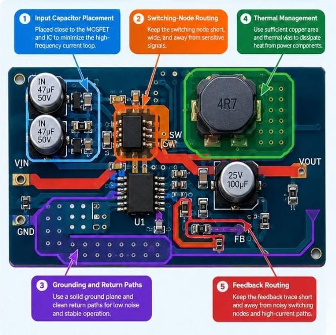
1️⃣ Input Capacitor Placement
The input bypass capacitor should be placed close to the switching regulator's input and power-switching stage, following the IC manufacturer's recommended layout.
Poor placement increases the high-frequency current-loop area, potentially causing voltage spikes, ringing, and increased electromagnetic interference (EMI).
2️⃣ Switching-Node Routing
The SW node experiences rapid voltage transitions and can be a significant source of electromagnetic noise.
Keep this node appropriately sized and compact, and route it away from sensitive analog signals, feedback networks, and other noise-sensitive circuits.
3️⃣ Grounding and Return-Current Paths
Grounding is not simply about connecting every ground pin to a copper plane.
High-frequency return currents follow paths influenced by the circuit's impedance and reference planes. Poor return-path continuity can increase noise coupling and interfere with nearby circuitry.
A carefully planned ground structure helps maintain predictable electrical behavior.
4️⃣ Thermal Management
MOSFETs, regulators, diodes, and inductors can generate significant heat.
Copper area, thermal vias where appropriate, component spacing, and the thermal characteristics of the selected components all influence heat dissipation.
Poor thermal design can reduce efficiency, compromise reliability, and trigger thermal shutdown.
5️⃣ Feedback Signal Routing
The feedback network determines how the regulator senses and controls its output voltage.
Routing sensitive feedback signals near switching nodes or high-current paths can introduce noise into the control loop, potentially causing output ripple, poor regulation, or instability.
Keep feedback routing short and away from noisy regions, following the regulator manufacturer's layout recommendations.
What does this mean for hardware developers?
A PCB layout should not be treated as a cosmetic step after schematic capture. It is an essential part of power-supply engineering that influences performance, reliability, EMI, thermal behavior, and manufacturability.
At ADDIS PCB Design LLC, we believe reliable electronic products begin with thoughtful engineering decisions—from schematic design and component selection to PCB layout and manufacturing preparation.
Whether you're developing an industrial controller, an embedded device, a power-management circuit, or a new electronic product, our team can help you approach your hardware design with these considerations in mind.
Developing a hardware product? Let's discuss your PCB design requirements.